User Profile

RLee42
 Occasional Contributor
Joined 7 years ago


User Widgets
Contributions
Clock generated from normal IO has a DC offset
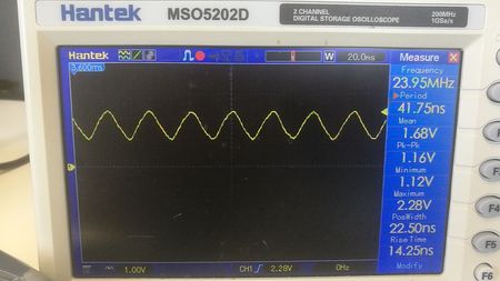
I tried to use general IO to generate a clock for other ICs. This generated clock is from the PLL which is fed in with a crystal oscillator. When I measured this clock at the output pin, I found that the frequency is correct as I expected, but the voltage is not correct. This pin is configured as LVCMOS-3.3v, so the Voh/Vol should around 3.2v/0.1v, but from this image below, the Max/Min voltage is 2.28v/1.12v. It has an above 1v DC offset which makes trouble for other ICs who use this clock. My question is how to reduce this DC offset to make the IO generated clock meet the LVCMOS standard.Solved1.9KViews0likes2CommentsRe: Timing constraints on between FPGA and external PLL
Hi Sstrell, Thanks for your replying. I'd like to provide more details for your reference. 4) false path the clock output path so it's not analyzed as a data path (set_false_path) ...How does this external device's PLL work? Can you just feed a 40 MHz clock through it without any changes? -- This DSP PLL is embedded in the DSP which can generate a local clock by multiplying the input reference clock. The original intention I used this PLL to generate 40Mhz from 20Mhz is to reduce the PCB layout timing restriction. Since 40Mhz would be easier for FPGA timing constraints as you suggested, I would try to use the 40Mhz clock between DSP and FPGA instead. 6(?) Not sure if that "interface ctrl" is outputting from the FPGA but if it is you'd need set_output_delay -max and -min as well -- Sorry that I haven't made it clear. The depicted Databus between Interface module in DSP and Interface ctrl module in FPGA includes a 16bit data bus and some other control signals to each direction, like R/W, cs, and ready, so I reckon the set_output_delay max/min constraints are also needed.2KViews0likes1CommentTiming constraints on between FPGA and external PLL
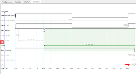
I'm using MAX10 to interface with a DSP. The FPGA is the clock provider whose PLL generated a 20Mhz clock to DSP and a 40Mhz clock(fpga_clk) for local use. The DSP uses DSP PLL to generated a 40Mhz local clock(dsp_clk) from the FPGA provided 20Mhz. Then the DSP uses this 40Mhz local clock(dsp_clk) to send parallel data/address to FPGA. Since FPGA and DSP use different PLL to generate their own 40Mhz clock, so my question is can FPGA use its local 40Mhz clock(fpga_clk) to directly fetch data from DSP generated with dsp_clk? Is there any cross clock domain process needed? If it's not needed, how would the timing constraints be set in this scenario? The timing parameter provided by the DSP datasheet includes the PLL input clock to output clock delay min/max value, the clock to output data delay.2.1KViews0likes4CommentsRe: question about dual-purpose pins used as normal I/O
Thank you for your reply. I've already hard-wired the nCONFIG, CONF_DONE pins to control other components as the output pins, and the nSTATUS pin as GPIO connecting with another MCU. They are already used as the user I/O on the PCB so I think that option may conflict with the hardware. However, I've made an experiment that I jumped wire the nCONFIG, CONF_DONE to 3.3v through 10k resistor, then the FPGA can run successfully after reboot. I think these two pins should better be left alone and pull-up for the next version.1.4KViews0likes1Commentquestion about dual-purpose pins used as normal I/O
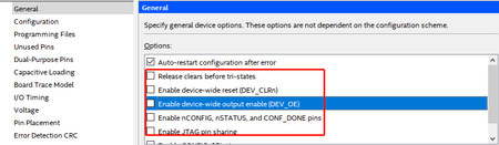
I'm using 10M08SAE144I7 for the new design. Since the normal IO number is not enough for this design, in order to add more IO, I disable all the dual-purpose pins in the device by unticking all the options for dual-purpose pins. I think in this way these pins can be used as normal IO. With this setting, I download .sof file to the FPGA, everything works fine. However, if I download .pof file into FPGA, the FPGA doesn't work at all after board reset. I guess maybe some dual-purpose pins can't be used as normal IO but not sure which ones are. Can you tell me which dual-purpose pins definitely can't be used as normal IO?1.4KViews0likes3CommentsRe: constraints on output clock
Thanks for your answer. I'm not quite sure about the 3rd constraint in your answer, so more explanation is appreciated. I've listed the related code below. This is PLL implementation, clk_out_40M is connected to a pin directly. PLL inst_PLL ( .areset(rst_n), .inclk0(clk_20M), .c0(clk_out_40M), .locked() ); This is constraints in .sdc create_clock -name {clk_20M} -period 50.000 -waveform { 0.000 25.000 } [get_ports {clk_20M}] derive_pll_clocks set_false_path -from [get_clocks clk_20M] -to [get_clocks clk_out_40M] What I can't quite understand is why should I add "create_generated_clock -multiply_by 1"? I think "derive_pll_clocks" in my .sdc file has already told the tool relation between clk_20M and clk_out_40M?2.5KViews0likes1Commentconstraints on output clock
My question is about how to generate a 40MHz clock from MAX10 as a clock source for another chip on PCB. What I have done is implementing a PLL with external 20Mhz crystal as the input and output c0 is configured to 40MHz. What I'm going to do is to connect this 40MHz pin to the clock port of another chip(CY7c68013). My question is: 1 . Can I assign any pin on MAX10 with PLL output c0 as output clock? Or I can only assign them to specific pins? 2. How would I add timing constraints on this output pin?Solved2.6KViews0likes3CommentsHow to deal with ADC pins of MAX10
It's my first time to use MAX10 ADC so I'm not sure whether my design can work. What I have already done is generated an ADC core and also a PLL core connected with it. On my PCB, the analog signals to be measured have already been connected to the ADC pins of MAX10 on BANK1A. However, I don't what kind of restrictions are needed for these ADC pins? Should I just simply leave these pins unused in the top module of my project or should I add some restrictions, like "reserved as input tri-stated" in assignment edit to let Quartus know these pins are allocated for ADC?Solved901Views0likes1Comment